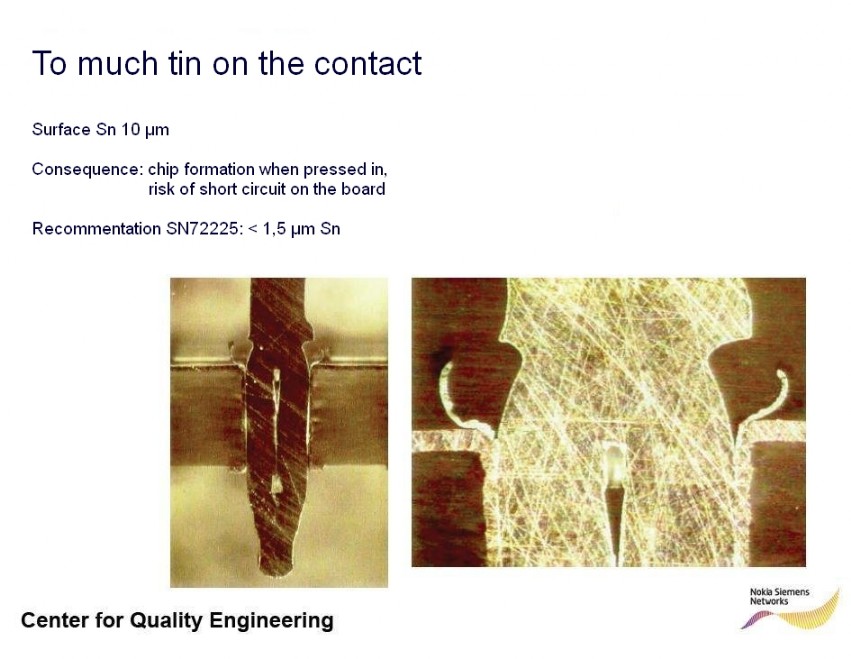

Tin thickness, chip formation
Tin chip formation or Tin abrasion
could be at some contact types, when too much Tin is applied in the hole or on the contact.
Are the Tin chips at the exit site of contact, they come from the tinning of the PCB. However, are they visible on the entry site they are abrasion from contact.
This frequently occurring abrasion can be avoided only if the tin coating on the contact is as thin as possible. From a Tin layer thickness greater than 1.5 µm, abrasion is inevitable.
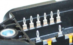
Some contacts need Tin as a "Lubricant" when pressed in.
Some contacts requires no Tin on the contact points. Also pre-tinned material therefore can be used, with bare punched edges.
A rapid insertion is then useful.
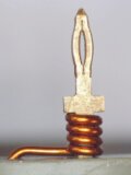
In the hole the contact should push all Tin to the side and not as chips to the front outside the hole.